
About photonic nanostructures
Photonic crystals
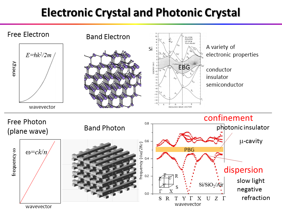
Photonic crystals are structures with a periodic modulation of the refractive index in the wavelength scale and can be fabricated by state-of-art equipment. In usual crystals, band structures are formed by a periodic potential produced by atoms. Similarly, in photonic crystals, photonic band structures appear in the photonic dispersion, resulting in unusual photonic materials, represented by the appearance of photonic band gaps and exotic dispersion, can be realized.
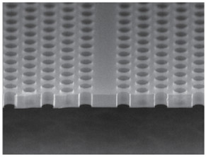
The hole radius is around 100 nm.
Examples of research topics in our team
・Negative refraction
Refractive index goes to negative and exotic lens can be realized.
・Slow light
Propagation speed of light can be controlled. The minimum speed is c/50,000
・Strong light confinement by a nano cavity
Confining light strongly in sub-wavelength region.
・Adiabatic wavelength tuning
Tuning of wavelength of light like strings of guitar.
・Ultra-small optical devices with ultra-low energy consumption
Promising for dense optical network into a processor chip.
Plasmonics and Metamaterials
Photonic crystals are made of dielectric materials, while metallic nanostructures also provide an exciting platform in nanophotonics. Usage of plasmons, cooperative oscillation of free electron in metal, realize strong confinement of light in several tens of nanometers and the research field using plasmon in nanostructures is called "Plasmonics." Moreover, metal nanostructures much smaller than wavelength can act as an electric circuit for photons, which is called "Metamaterials." Our team is exploiting also these plasmonic structures and metamaterials in parallel to photonic crystals.
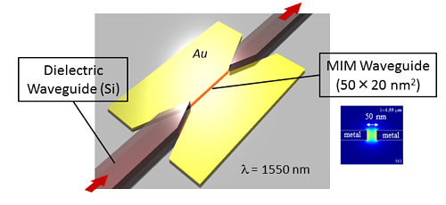
This MIM waveguide is coupled to a conventional dielectric waveguide with very high coupling efficiently and can focus the light into an area with 1/2,000 of light wavelength.
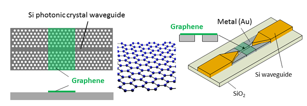
Fusion of Nanomaterials and Nanophotonics
Recently, nanomaterials such as graphene, TMDC (transition metal di-chalcogenide), carbon nanotube, and nanowire, are intensely investigated because of their exotic physical properties. They exhibit various interesting electronic and optical properties, but their light-matter interactions are severely limited because of their small interaction cross-sections. To overcome this issue, our lab. is establishing new optical platforms to enhance the light-matter interaction and exploring novel optical phenomena by combining nanomaterials and nanophotonics. (科研費基盤S「ナノマテリアル・ナノフォトニクス融合による新しい光集積技術の創製 」(H28-H32))
(Formation of an optical cavity is controllable due to gate control)
Right: Graphene loaded plasmonics MIM waveguide
(Enhancement of ultra-fast-nonlinear-effect in graphene)
Fusion of Solid state physics and Nanophotonics
Photonic crystals are a photonic version of conventional electronic crystals well-studied in solid state physics. Recently, research fields using another analogy between electrons and photons are becoming very active.
One example is a topological insulator which won Nobel prize of 2016.
This is a new electronic property resulting from topological nature in electronic band structures.
Sililarly, photonic crystals with special class of geometric properties have been shown to possess interesting topological nature and realize unusual optical phenomena, which is now being discussed energetically in optics community.
Valleytronics, new technology using valley degree of freedom of electrons in semiconductors, especially in two dimensional materials, is a hot research area. Recently, its photonic analogy (photonic valleytronics) is attracting much interest and various interesting properties have been demonstrated.
It was pointed out theoretically that non-Hermitian system with parity-time (PT) symmetry can have real eigenstates, and later this phenomenon was demonstrated in optics by employing materials having both gain and loss. Recently, various unusual interesting phenomena were found in PT-symmetric optical systems at around the transition point of the PT symmetry, such as non-reciprocal reflection and superluminal light propagation.
Our Lab. is pursuing these topics by fully utilizing nanofabrication technologies, especially for photonic crystals.
Toward optical computing
Optical computing was intensely investigated from 80's to 90's, however, declined due to great progress of CMOS processors. Recently, we claimed the possibility that optical computing can show advantage against CMOS processing, especially about latency, if we fully make use of nanophotonics technology and are exploiting basic research toward optical computing. (Although this project is mainly being done in NTT Lab with support from JST-CREST, our Lab. also will contribute it.)


